What are the details of your FR4 material?
- High Glass Transition Temperature (Tg) (150Tg or 170Tg)
- High Decomposition Temperature (Td) (> 325º C)
- Low Coefficient of Thermal Expansion (CTE) ((3.0%-3.8%)
- Dielectric Constant (@1 GHz): 4.25-4.55
- Dissipation Factor (@ 1 GHz): 0.016
- UL rated (94V-0, CTI = 4)
- Compatible with standard and lead-free assembly.
- Operating temperature is 125 degrees C.
While the laminate has a UL flammability rating UL rated (94V-0, CTI = 4), we do not stamp a UL rating on the boards. As a result, the boards that we manufacture are not UL rated.
Do you offer PCB Assembly?
Can I share my custom components with others?
ExpressPCB Resources
PCB MFG Aids
Stevens Products Inc.provides edge protectors, Gold Finger Gloves, PCB Stiffeners, PCB Carriers, etc. Check out their products!
Submitted by our cool customer: Peter Capobianco “…audiophile and tube hi-fi DIYer extraordinaire…”
https://stevensproducts.net/products.htm
PCB Trace Width Calculator
This Javascript web calculator calculates the trace width for printed circuit boards based on a curve fit to IPC-2221 (formerly IPC-D-275).
https://circuitcalculator.com/wordpress/2006/01/31/pcb-trace-width-calculator/
PCB Via Calculator
This Javascript web calculator calculates the resistance, voltage drop, and power loss of printed circuit board vias. Note that vias are made out of plated copper which typically has a resistivity of 1.7E-6 to 2.2E-6 Ohm-cm. The calculator has an input box for the resistivity which defaults to 1.9E-6 Ohm-cm.
https://circuitcalculator.com/wordpress/2006/03/12/pcb-via-calculator/
Tektronix TDS-1000
The Tektronix TDS-1000 is a great low-cost digital storage oscilloscope for the microprocessor developer. We have the old model TDS-220 and love it. The ability that storage scopes have to capture and display a single event make them extremely handy for micro controller development. This model’s very compact size also makes it great in the field. We do however consider that an analog scope may still be a better choice for doing sensitive analog work. These scopes are somewhat noisy at low voltages.
Mitutoyo Calipers
When laying out PC boards, it is very useful to measure small distances accurately. Selecting hole sizes for components requires measuring pin diameters in thousandths of inches. When placing pads for components or connectors with unusual lead spacing, it is necessary to carefully measure the pin layout. We have always been happy with Mitutoyo calipers for this job. We use both their dial and digital display models. A good selection of Mitutoyo calipers are available at McMaster-Carr. For the casual user, a no-name brand dial caliper is likely to be fine and cost under $50.
Digi-Key
Digi-Key is a great resource for electronics components, such as semiconductors, resistors, capacitors, and connectors. They have a large inventory and ship very quickly. Their catalog often shows physical dimensions of parts, which is a big help when laying out PC boards. Many parts found in the ExpressPCB component library include Digi-Key part numbers. products!
Mouser Electronics
Mouser Electronics is very useful source for electronic components, particularly when prototyping. Their website and online catalog is an important source of technical information such as component data sheets.
Pic-Servo Motion Control
We find that motion control projects are made easy using the PIC-SERVO. The PIC-SERVO is available either in a two chip set, or as a single board controller that includes the motor amplifier. It has a serial interface so it is easy to connect with a computer. The PIC-SERVO is probably the fastest and least expensive way to get a DC servo motor up and running. They also offer a stepper motor controller.
GetThePatent.com
If you are considering patenting a new invention or product, a great place to start your research is GetThePatent.com. They offer a fast online tool for patent searches. Their database not only includes US patents, but also the patents registered in most European countries and Japan.
Envision Plastics
Envision Plastics and Design offers an interesting enclosure solution for products to be manufactured in quantities from 50, up to a few thousand. Their plastic enclosures have a “consumer product” feel, but do not require expensive tooling or setup costs. This makes them a practical solution for small production runs.
Alta Via Technologies
Alta Via Technologies is a high-end PCB design service. They specialize in laying out complex circuit boards for commercial, military, and medical applications. They offer significant expertise when working with PCB design issues such as high speed circuits (10Ghz +), high density SMT packages, and controlled differential impedance.
McMaster-Carr Supply
McMaster-Carr Supply Company is a good source for mechanical parts. They have a complete selection of screws, nuts, washers and other fasteners. McMaster’s offers raw materials such as aluminum and plastics. They are also a good source for tools and machine shop supplies. They almost always have what you need in stock and ship very quickly.
Online Metals
Online Metals is a very convenient source for purchasing small amounts of machinable metals and plastic. They have a good selection of aluminum in both sheet and plate, as-well-as delrin, nylon and acrylic. They will also cut to size.
AppCAD
AppCAD is a free RF design tool for Windows that can be downloaded at no cost from HP / Agilent. It is useful to help with the calculations for many RF, microwave, and wireless applications. PC board designers of RF circuitry will find the transmission line calculator handy. It also includes many computerized application notes relating to RF topics.
Can I order Production Service with no soldermask?
Yes.
To ensure no soldermask on the top or bottom layer, use the
rectangle tool to mask out the soldermask for the entire board on both
the top and bottom soldermask layers.
Go to View Options
Select “View Top Soldermask Layer”:
Use the rectangle to cover the entire board.
Do the same for bottom solder mask layer.
How do I reorder my ExpressPCB design?
If you would like to reorder boards, the procedure
is the same as when they were ordered the first time. All orders must
be placed using the ExpressPCB program. Be sure to have the .PCB file
loaded that you would like to order.
Will you quote my Gerber files or files from other design tools?
Unfortunately our manufacturing service is only available to orders from our ExpressPCB design software.
For manufacturing orders from Gerber files we recommend you try EasyPCBUSA.com,
they utilize the same PCB manufacturer as we do, so we can vouch for
the quality and on time delivery, it will be second to none. The
online quote form is very easy to use. They can be reached at Support@EasyPCBUSA.com if you have questions.
We have partnered with Sunstone Circuits to provide quality PCBs
made in the USA for 20 years. They accept native files from several
different PCB Design applications as well as Gerber files, and can
provide a more expansive array of manufacturing options. You can visit
them at https://www.sunstone.com or contact them at support@sunstone.com.
Can I have my ExpressPCB design converted to Gerber files?
You can now request gerber files right from our
software when ordering your PCBs! There is no longer any additional fee
to request gerber files with your order. We do not currently offer
gerber files without an order for PCB manufacturing.
We will then email the gerber files back to you as an attachment with your tracking number when your boards are shipping.
You will receive these files:
+ Top silkscreen layer
+ Top solder paste layer
+ Top soldermask layer
+ Top copper layer
+ Bottom copper layer
+ Bottom solder paste layer
+ Bottom soldermask layer
+ Drill file
+ 4 layer designs also include the 2 inner layers
+ Pick and Place Files
Will you design my circuit board for me?
We do not provide design services for creating circuit boards.
Making Schematic Components For ExpressSCH
Making Custom Schematic Components From Scratch
The ExpressSCH program includes hundreds of components and symbols that you can use to draw your schematics. However, sometimes we may not have all of the parts that you need. In these cases, you can easily create your own. This guide describes the simple steps of how to make schematic components and also provides tips on giving them the same appearance as those found in our library.
The procedure for making new components with ExpressSCH is very easy. The general, idea is to draw the new part right in your schematic using rectangles, lines and arcs. At the locations where external wires will attach to the component, pins (shown as small dots) are placed. Then all of the rectangles, lines, arcs and pins are grouped together, creating a “component”. Here are the steps:
Designing Components For a Standard Appearance
We recommend designing your custom components so that they have the same overall appearance as those found in our library. By doing that, a schematic drawn with a mixture of our library components and your special components will maintain a professional appearance.
Many integrated circuits having numerous pins are drawn as a simple rectangle with lines for each lead. Because they can be very large, make a effort to keep them compact, but also readable and neat. We recommend setting the snap-to-grid to 0.05″ and using these dimensions when drawing rectangular components:
| The width of this component is shown as 0.9 inches. For components having many more pins and long pin names, a larger width can be used. For example, the component ATS908515 in our library has a width of 1.4 inches. |
After placing the pins (shown below as small dots) at the ends of the lines on the component, double click on each one to assign its Pin number and Pin name in the Pin Properties dialog box. In the same dialog box, selecting a text height of 0.060″ will give the printed pin number and name text the same appearance as we use.
Once the Pin number and Pin name values are set, you will need to drag their text to the desired locations. Before positioning the text, we recommend setting the snap-to-grid to 0.025″ .
| With the snap set to 0.025″, the Pin numbers are placed such that they sit about 0.006″ above the pin and 0.025″ from the edge of the component.The Pin name text is positioned so that it is centered vertically with the pin and about 0.035″ from the component’s edge.The pin numbers and name are also positioned so that the text is justified along the edge of the component. |
It is our conventions to place the power lines at the top of the component and the ground lines at the bottom.
The last step in creating a component is to group all of its parts together using the Group to make component command. This command will display the Component Properties dialog box where the Part name (i.e. AT90S2313) and Part ID (i.e. U12) is set. When creating an IC component that is to be added to your library, the Part ID is usually set to just U, then the number following the U is added later.
Once the Part name and Part ID values are set, you will need to drag their text to the desired locations. We recommend setting the snap-to-grid to 0.025″ before positioning the text.
| Here you can see that the U is placed near the upper left corner of the component and the Part name is placed in the middle. The orientation of the Part name text (set in the Component Properties dialog box) is set so that it reads from top to bottom. |
Naming Components and Saving Them
After a component has been created, you will want to save it in your component library. Once saved, it will then appear in the list of Custom components shown in the Component and Symbol Manager dialog box.
To save a component, select the Save custom component command from the Component menu. At this point, you will be asked to enter a name for the new component. You can enter any name you like, however the name can not be longer than 61 characters and can not include these symbols:
/ \ : * ? ” < > |
When entering the name, we recommend using the same naming standard that we use. By following our convention, your names will be arranged in the Component Manager dialog box in the same order as ours. Below are the guidelines for our naming convention.
We begin component names with a Component category. Here are the ones we use:
Connector – for connectors
IC – for integrated circuits
Misc – for batteries, relays, motors…
Passive – for resistors, capacitors, inductors…
Semiconductor – for transistors, diodes, LEDs…
Switch – for switches and buttons
Following the “IC” Component category, we generally add an abbreviated name of the IC manufacture. These are examples of the abbreviations we use:
| AMD –Allegro –Analog devices –Atmel –Burr Brown –Dallas Semi –Fairchild –Fujitsu –Hitachi Semi –Intersil – | Linear Technology -Maxim –Microchip –National –OKI –Philips Semi –ST Micro –TI –Toshiba – |
Next, the component’s part number is added. Letters in the part number are written in upper case. Following the part number, a short description of the part can optionally be added. Here are a few examples:
LM4861 – Amplifier
LM7805 – Regulator
AT90S2313 – Microcontroller
MAX873 – Voltage reference
Note that only the first letter of the description is in upper case and the words are separated by spaces.
In some cases a component package type is added to the end of the name. This is done when a component is available in multiple packages, each having different pin numbers. These are examples of a few of the package type abbreviations that we use:
DIP-40
PLCC-44
QFP-64
SOIC-20
SSOP-28
It is very important when picking package type, that the name be based on the package name used in the ExpressPCB program. Double check within the ExpressPCB program to verify that the package name you have selected has pad sizes and spacing appropriate for your component.
______________
Here are several examples of component names using the ExpressSCH naming convention with all of the fields discussed above:
IC – AMD – AM29DL322 – Flash memory
IC – Maxim – MAX232 – Line driver receiver
IC – National – LM7805 – Regulator – TO-92
IC – National – LM7805 – Regulator – TO-220
IC – Atmel – AT90S8515 – Microcontroller – PLCC-44
IC – Atmel – AT90S8515 – Microcontroller – DIP-40
Modifying Components From Our Library
In some cases, it is fastest to build a new component by starting with a close fit from our library. In other cases it is handy to make simple changes to one of our library components so that its appearance is better suited for your schematic. For example, you may want to rearranging the order the pins.
Modifying a component from our library is easily done by first inserting the component into your schematic. Next select the component with the mouse and then ungroup it using the Ungroup component command from the Component menu. Now move things around or make any other changes you wish using the methods described above. Finally, regroup it back together to create the new part using the Group to make component command.
The changes that you make will not affect the original part in our ExpressSCH library.
Creating Components With Multiple Gates
Some integrated circuits have multiple gates in one chip. For example a 74LS32 TTL component includes four OR gates in a 14 pin DIP package. Here is the procedure for creating schematic symbols that have multiple gates in a single package:
- Create the first gate using the steps listed above in the Making Custom Schematic Components From Scratch The first gate should include the power supply and ground pins.
- Assign the pin numbers to each pin on this first gate.
- Group the first gate together by selecting its pieces and choosing the Group to make component
- In the Components Properties dialog box, fill in the Part name field with the IC name (i.e. 74LS32) and assign the Part ID field to U.
- Create each of the remaining gates one at a time, grouping them individually using the same steps 1 through 4. On these gates, do not include the power pins. Each gate should have the Part ID set to U and have the same Part name as the first.
- After all of the gates have been created, save them in your library as a single component. Do this by selecting all the gates with the mouse and then choosing the Save custom component command from the Component
Here is an example showing a 74LS32 with its four OR gates:
| Note that only the first gate includes the power and ground lines, shown as pins 14 and 7. Each of these four gates have been created individually. That way they can be moved around independently in a schematic. However when the component is saved in the library, all four gates that make up one IC package are saved together.When a component with multiple gates is selected from the library and inserted into your schematic, all of the gates will be added at once. Feel free to position each gate individually in the schematic. Be sure to set the same Part ID value for each gate. Keep in mind that the Part ID represents the package, not the individual gate. For example these four gates might all have their Part IDs set to U7. |
Custom Component Files
When a component is saved using the Save custom component command, it is saved in an individual file on your computer and has a .S extension. The name of the file is the same as the one you entered when naming your component. You can find these files in a subdirectory where the ExpressPCB software is installed. Typically ExpressPCB and ExpressSCH are installed in the directory:
C:\Program Files\ExpressPCB
If this is where you installed our software, then you will find your custom components in the directory:
C:\Program Files\ExpressPCB\SchComponents_Custom
Feel free to move the component files that you have created from one computer to any other where ExpressSCH is installed. Of course we also recommend that you backup these files for safe keeping.
Documentation
Tips for Designing PCBs
The engineers at ExpressPCB have assembled a few general rules-of-thumb that can help beginners design their first circuit board. These tips are not specific to using our CAD software, but instead provide an overview to help explain how to position the components on the board and how to wire them together.
Placing Components
Generally, it is best to place parts only on the top side of the board.
When placing components, make sure that the snap-to-grid is turned on. Usually, a value of 0.050″ for the snap grid is best for this job.
First place all the components that need to be in specific locations. This includes connectors, switches, LEDs, mounting holes, heat sinks or any other item that mounts to an external location.
Give careful thought when placing component to minimize trace lengths. Put parts next to each other that connect to each other. Doing a good job here will make laying the traces much easier.
Arrange ICs in only one or two orientations: up or down, and, right or left. Align each IC so that pin one is in the same place for each orientation, usually on the top or left sides.
Position polarized parts (i.e. diodes, and electrolytic caps) with the positive leads all having the same orientation. Also use a square pad to mark the positive leads of these components.
You will save a lot of time by leaving generous space between ICs for traces. Frequently the beginner runs out of room when routing traces. Leave 0.350″ – 0.500″ between ICs, for large ICs allow even more.
Parts not found in the component library can be made by placing a series of individual pads and then grouping them together. Place one pad for each lead of the component. It is very important to measure the pin spacing and pin diameters as accurately as possible. Typically, dial or digital calipers are used for this job.
After placing all the components, print out a copy of the layout. Place each component on top of the layout. Check to insure that you have allowed enough space for every part to rest without touching each other.
Placing Power and Ground Traces

After the components are placed, the next step is to lay the power and ground traces. It is essential when working with ICs to have solid power and ground lines, using wide traces that connect to common rails for each supply. It is very important to avoid snaking or daisy chaining the power lines from part-to-part.
One common configuration is shown below. The bottom layer of the PC board includes a “filled” ground plane. Large traces feeding from a single rail are used for the positive supply.
Placing Signal Traces
When placing traces, it is always a good practice to make them as short and direct as possible.
Use vias (also called feed-through holes) to move signals from one layer to the other. A via is a pad with a plated-through hole.
Generally, the best strategy is to lay out a board with vertical traces on one side and horizontal traces on the other. Add via where needed to connect a horizontal trace to a vertical trace on the opposite side.
A good trace width for low current digital and analog signals is 0.010″.
Traces that carry significant current should be wider than signal traces. The table below gives rough guidelines of how wide to make a trace for a given amount of current.
0.010″ 0.3 Amps
0.015″ 0.4 Amps
0.020″ 0.7 Amps
0.025″ 1.0 Amps
0.050″ 2.0 Amps
0.100″ 4.0 Amps
0.150″ 6.0 Amps
When placing a trace, it is very important to think about the space between the trace and any adjacent traces or pads. You want to make sure that there is a minimum gap of 0.007″ between items, 0.010″ is better. Leaving less blank space runs the risk of a short developing in the board manufacturing process. It is also necessary to leave larger gaps when working with high voltage.
When routing traces, it is best to have the snap-to-grid turned on. Setting the snap grid spacing to 0.050″ often works well. Changing to a value of 0.025″ can be helpful when trying to work as densely as possible. Turning off the snap feature may be necessary when connecting to parts that have unusual pin spacing.
It is a common practice to restrict the direction that traces run to horizontal, vertical, or 45 degree angles.
When placing narrow traces, 0.012″ or less, avoid sharp right angle turns. The problem here is that in the board manufacturing process, the outside corner can be etched a little more narrow. The solution is to use two 45 degree bends with a short leg in between.
It is a good idea to place text on the top layer of your board, such as a product or company name. Text on the top layer can be helpful to insure that there is no confusion as to which layer is which when the board is manufactured.
Checking Your Work
After all the traces are placed, it is best to double check the routing of every signal to verify that nothing is missing or incorrectly wired. Do this by running through your schematic, one wire at a time. Carefully follow the path of each trace on your PC layout to verify that it is the same as on your schematic. After each trace is confirmed, mark that signal on the schematic with a yellow highlighter.
Inspect your layout, both top and bottom, to insure that the gap between every item (pad to pad, pad to trace, trace to trace) is 0.007″ or greater. Use the Pad Information tool to determine the diameters of pads that make up a component.
Check for missing vias. ExpressPCB will automatically insert a via when changing layers as a series of traces are placed. Users often forget that via are not automatically inserted otherwise. For example, when beginning a new trace, a via is never inserted. An easy way to check for missing via is to first print the top layer, then print the bottom. Visually inspect each side for traces that don’t connect to anything. When a missing via is found, insert one. Do this by clicking on the Pad in the side toolbar; select a via (0.056″ round via is often a good choice) from the drop down listbox, and click on the layout where the via is missing.
Check for traces that cross each other. This is easily done by inspecting a printout of each layer.
Metal components such as heat sinks, crystals, switches, batteries and connectors can cause shorts if they are placed over traces on the top layer. Inspect for these shorts by placing all the metal components on a printout of the top layer. Then look for traces that run below the metal components.
ExpressPCB Plus Schematic Link
With ExpressPCB Plus version 3.0.3 we have introduced the Schematic Link tool, similar to our Classic software. This feature will allow a netlist from ExpressSCH Plus to be linked with a layout in ExpressPCB Plus. This is a basic comparison of component names and pins that allows users to highlight connected pins in the layout to assist with routing the physical connections in the design.
To begin, users will create a schematic in ExpressSCH. The most critical detail will be the use of identical component names and pin numbers. Pin numbers are either set prior to grouping elements to create a component, or already labeled within a saved part.
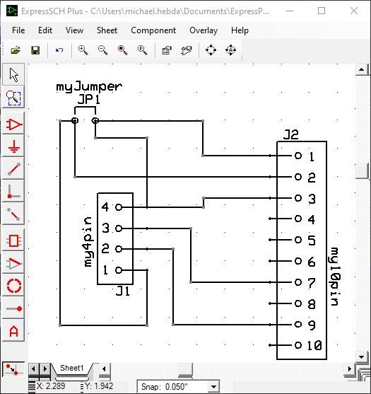
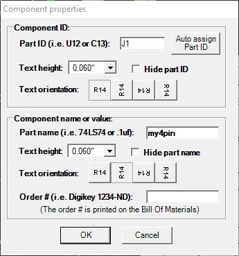
Once a part is selected, you can right click and chose Set Component Properties to verify the component name and ID, and make any necessary changes.
When the schematic is finished, it is helpful to run the "Check schematic for netlist errors", which is found in the File menu. This will check for duplicate component names or pin numbers, as well as wires that may not connect with pins completely. Once finished, the schematic is saved, and work begins in Plus to create the layout.
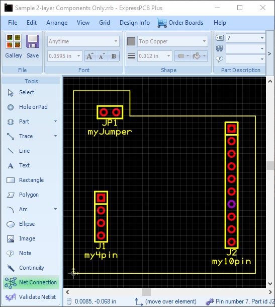
Below is a sample design with the same components as shown in the schematic previously:
By selecting a component, you will be able to view and edit the Component Properties in the ribbon menu at the top of the work area:
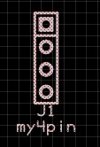

By clicking a second time on a particular pin. you can then view or edit the pin properties in the same portion of the ribbon menu:


Once the components and pins have been placed in ExpressPCB Plus, the "Link Schematic to PCB" command can be run from the File menu. This will open an Explorer window, allowing you to browse and select the correct schematic file. When completed, you will receive a pop-up message:
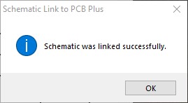
There will be subsequent messages informing you the schematic netlist can be used for Netlist Validation as well. If the schematic you chose contains Symbols, this will generate a default error for each symbol:
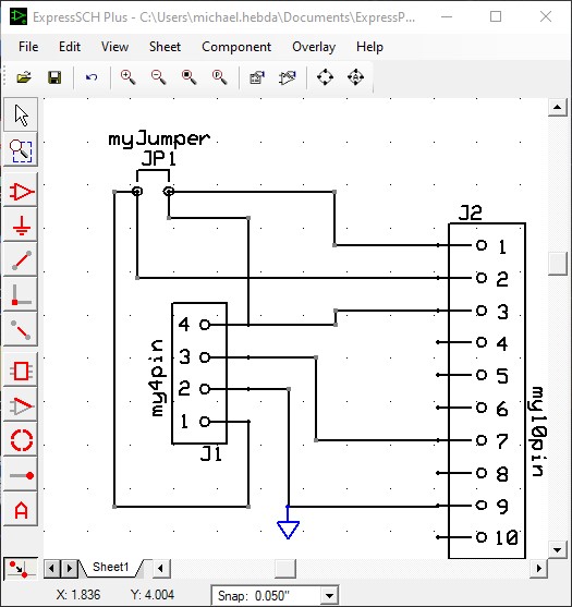
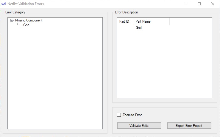
At this time, the Symbols Properties in ExpressSCH have a Net Name:
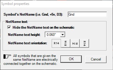
The concept of Net Names is not yet supported in ExpressPCB Plus, but is on our development map. You may chose to disregard errors related to Symbols at this time, or have an alternate version of the SCH file with the symbols removed.
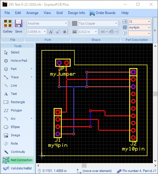
In either case, the Schematic Link will function. Once the SCH file is linked, click on the "Net Connection" tool from the Tools menu at lower left of the work area. The cursor will change from the Select Arrow, to an Electrical Probe. Clicking on a pad in the layout, will then highlight all of the connected elements found in the schematic netlist similar to below:
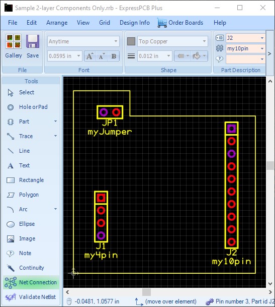
If your schematic contains a symbol such as my Schematic with Symbol above, with a GND symbol connected to J1 pin 2 and J2 pin 9; you will still find the connected pins highlight correctly:
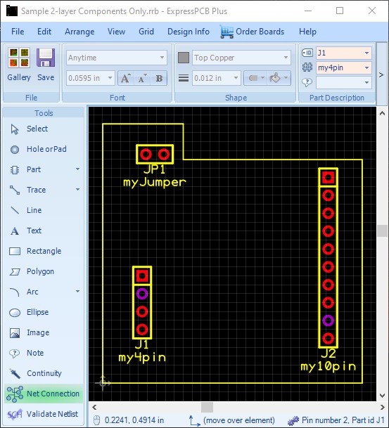
However, there will be a message regarding the symbol:
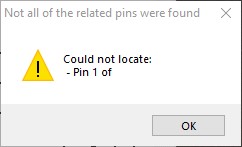
Click OK to close the message, and connections can then be placed as needed between the highlighted pins.
If you would like a different color for either your layers or the Schematic Highlight, click on the View menu and select "Layer Colors and Visibility". An interface will open, allowing you to left click on the color box of the layer you wish to change. Simply choose the color you would like, and click OK to update.
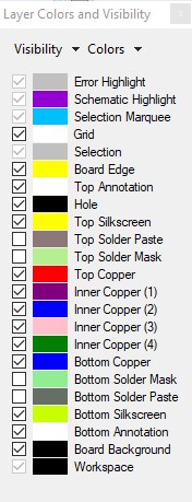
The Net Connection tool will continue to function as you complete your design, showing the connected pads in a unique color from any additional errors or selection highlights. The following is an example of the Net Connections highlight the pads in purple, while the Continuity tool highlights the traces and vias connecting them in a different manner:
We hope this helps provide the necessary steps to help with the Schematic Link tools and messages. If you need any additional information or assistance, please contact us with our Live Chat during Support Hours of 7:30am - 5pm Pacific Time, or by e-mail: support@expresspcb.com.
Netlist Validation in ExpressPCB Plus v3.0
With an ever increasing level of technology, we felt it was important to build off the schematic link, and provide additional verification of the final layout to the schematic. With the new Validate Netlist tool, ExpressPCB Plus will compare the current layout with netlist from the Schematic Link to determine if they are equivalent.
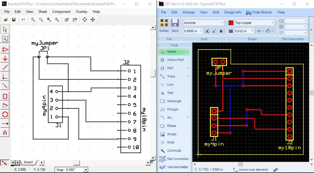
To begin, one needs a schematic from ExpressSCH Plus, and a layout in ExpressPCB Plus. In the sample shown below, we have a layout with several different errors to demonstrate the findings and reporting:

At the bottom of the Tool menu, towards the lower left of the Plus window, click on the "Validate Netlist" command. If you have already linked a schematic, you will receive a prompt to either use the current one, or link a different SCH file of your choice. Click OK to run, if potential issues are found, they will be shown in the following manner:
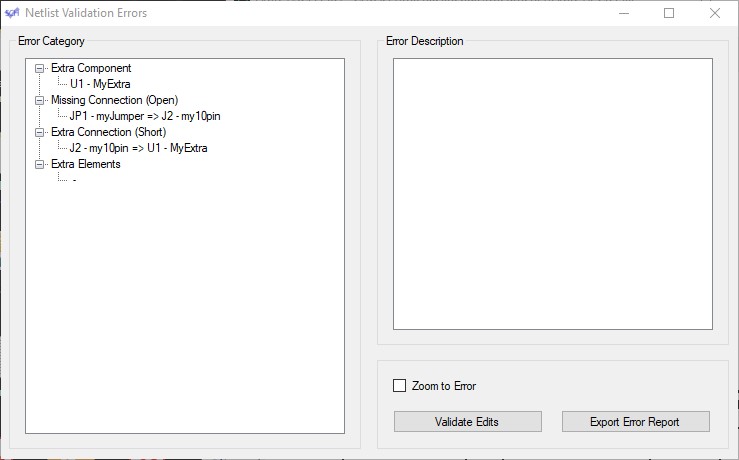
You may click on the header for each of the error types present to expand the list of items found. By clicking on a particular error, you will see the details of the error populate the right side with part/pad information, and the location of the error:
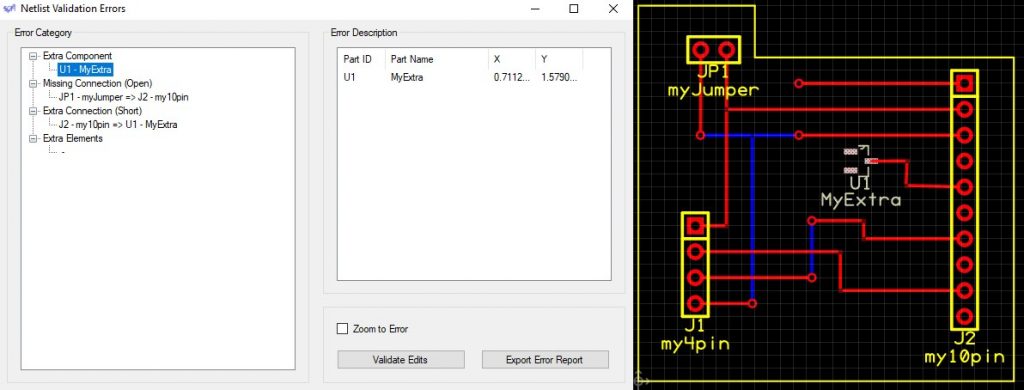
You may choose to toggle the "Zoom to Error", which will adjust the zoom level to display the error location instead of the current display level. Selecting the different errors will change the highlight, and potential zoom location depending on your selections.
For missing connections, the pads connected in the schematic file will be highlighted for you to determine where traces or connections to plane are missing:
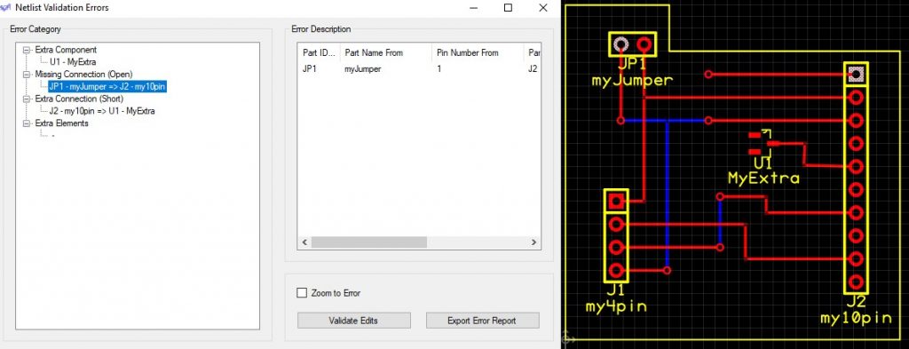
Any extra connections (electrical shorts) will display the pads and routing that create a connection not found in the schematic.
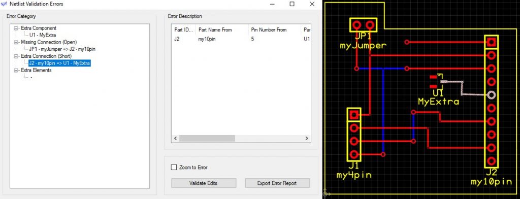
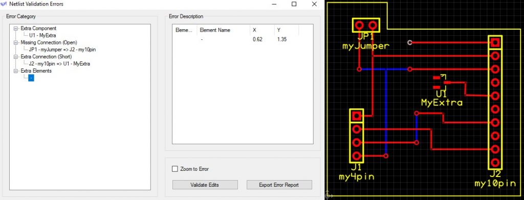
The last item we report on are extra elements that may not needed, or may be the result of a missing connection. These may not be shown in the same manner, as vias or connective pads/holes do not have explicit name or pin numbers. The following error is an example that results from the removal of a trace on the bottom layer connecting pins 1 and 3 of component J2:
If you would like to document the errors found, or need an alternate means to provide data, we have also included an "Export Error Report" feature. Clicking on this button will export the error data into a Microsoft Excel formatted file. (Please note, this functionality requires the user to have a licensed and functioning copy of Excel.) Below is a sample of the output file:

Once you are able to resolve the errors, either in the schematic or the layout, clicking on the Validate Edits button will process the "Validate Netlist" command again.
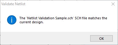
Once the files are equivalent, you will receive the following pop-up message:
We are excited to present this netlist validation to our users, and hope this provides the necessary steps to utilize this feature. If you need any additional information or assistance, please contact us with our Live Chat during Support Hours of 7:30am - 5pm Pacific Time, or by e-mail: support@expresspcb.com.
How do I change the number of copper layers in my design?
In ExpressPCB Classic and Plus, a new design defaults to two copper layers. If you find your design requires more copper layers, this can be changed with the Board Properties. This process can also be used to reduce the number of copper layers used if you find they are unnecessary as your design progresses.
In ExpressPCB Plus, this can be found in the Design Info menu:

Once you click on the board properties, there will be a number of items available to change as needed. To add more layers, simply click on the drop down menu for Copper Layers and select the number your design requires:

For ExpressPCB Classic the process is almost identical, though it starts with the Layout menu:

Selecting the Board Properties will open the following window:

ExpressPCB Classic is limited to just two or four copper layers. If you require additional layers, ExpressPCB Plus would be the appropriate software. Designs started in ExpressPCB Classic can be imported into ExpressPCB Plus. Please note, any changes made can not be imported back to Classic, as the software is not backwards compatible.
If you need any additional information or assistance regarding how to change the number of layers or board properties, please contact us with our Live Chat during Support Hours of 7:30am - 5pm Pacific Time, or by e-mail: support@expresspcb.com.
How do I modify the board outline in ExpressPCB Plus, and what does it effect?
In ExpressPCB Plus, the outline defines both the board edge, as well as the internal plane for inner layer copper on 4 or 6 layer designs. If you click and hold the left mouse button on the Board Edge, you can drag and drop the outline. Please note this does not move the design components or trace routing, but only effects the board edge and defined plane associated with inner layers.
If you click a second time to highlight a single edge or corner point, holding the left mouse button will then allow you to drag and drop the selected element. If you wish to add an additional point(s), you can either double click on a board edge to place the point, or right click and select "Add Point" from the item menu that pops up:

Once the point is added, a darker square will appear along the line segment of the board edge. An example is circled on the left edge in the image below:

With ExpressPCB, it is important to note that our standard router requires 0.100" spacing between edges. If your design requires a key slot, a notch in the board edge, or you nest several PCB's into one design layout; a minimum of 0.100" spacing will ensure your board is routed as you expect. The example below demonstrates a 5 board set, utilizing 0.100" spacing (as shown in the displayed grid pattern):

One additional aspect of the Board Edge is our built in Design Rule Check (DRC). While it is possible for silkscreen or even copper to overhang the board edge, there are additional checks for holes to close to the board edge or elements outside the board edge. The DRC is automatically run when placing an order to manufacture your design, and may potentially show areas that need to be edited and saved prior to placing the order.
We hope this helps to explain how the board edge is used in ExpressPCB Plus, and how edits can be made to meet your design needs. If you need any additional information or assistance, please contact us with our Live Chat during Support Hours of 7:30am - 5pm Pacific Time, or by e-mail: support@expresspcb.com.
How to create SMT pads with solder mask opening, versus copper covered with mask
Placing a pad in ExpressPCB Plus is an easy and straight forward task, however some design requirements such as heat sinks may not require all areas of copper to free of solder mask. For surface mount technology (SMT) pads, our "Hole and Pad" interface in the ribbon task bar (found just above the workspace) is both easy and customizable for your needs.

There are a variety of pad shapes, both with and without holes. We do provide a preset list of sizes for each option, but users are able to click and edit the dimensions as needed

To place either a pad or a rectangular polygon, the icons are found in the toolbar on the left side of the work space (shown below with red dots indicating these specific items):

In the following example, I have added both SMT pads and rectangular polygons:
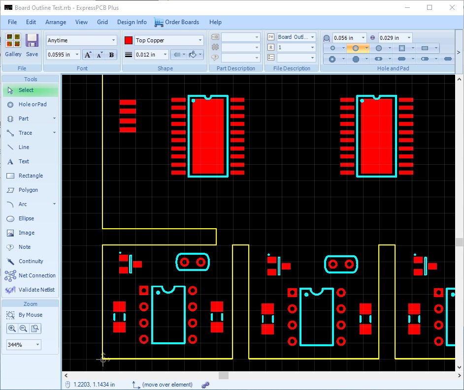
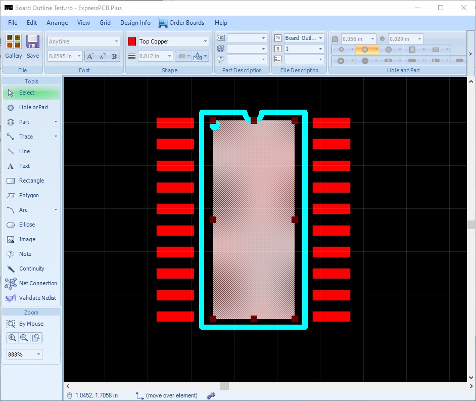
Upon initial placement, both look identical; which can lead to potential issues when sent to manufacturing as a result of their impact on the solder mask layer. You can select on these elements to help determine which type they are as shown in the two examples below:

To see the overall impact on the design, and understand how each type influences the solder mask layer; you can turn the solder mask layer on in the View menu, selecting "Layer Colors and Visibility", and checking the box for display. Below are examples of the solder mask layer and the difference between an SMT pad and a rectangular polygon:
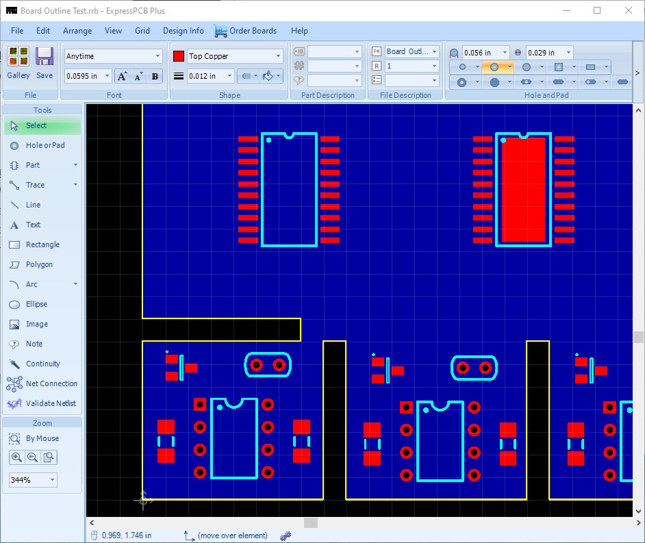

We hope this helps to distinguish these two methods of placing copper on your design, and how they differ to allow more options for your design. If you need any additional information or assistance, please contact us with our Live Chat during Support Hours of 7:30am - 5pm Pacific Time, or by e-mail: support@expresspcb.com.
How are the various polygon options used in ExpressPCB Plus, and what are their differences?
ExpressPCB Plus is designed to provide users with the options and flexibility they need in today’s workplace. One of the key features is designing with the use of copper pour (planes). Placing a copper pour can be done with a variety of commands from the toolbar on the left side of the work space: Rectangle, Polygon, Arc, or Ellipse.

Copper pour is also the default for all inner layers in ExpressPCB software. You can select “Pour” from the top ribbon toolbar, in the Pour Options Drop Down Menu:

Placing a pour will automatically adhere to the Pour Clearance properties of your design. You can right click on specific selected element(s) in your design and select Pour Clearance to adjust these settings if different spacing is required between design elements and copper pour:

You can also select a component or specific pads in a component or your design, right click and select Pad Connections to Pour and choose which layers they connect to and how:

Placing a rectangle and selecting “Outline” from the Pour Options drop down menu will place a solid rectangle using the trace width specified in the size drop down also found in the Shape ribbon toolbar. This will solidly connect to any elements it crosses, and is not affected by the pour clearance settings:

Selecting the “Fill” option will place a solid filled element that also solidly connects any elements within the boundaries of the rectangle, polygon, etc. and is not affected by the pour clearance settings:

Selecting the “Pour” option is the one affected by the Pour Clearance and Pad Connections settings. You will note Pin #20 has the Thermal connection toggled, and is connected accordingly, while all other elements within the boundary of the rectangle have clearances as designated:

This behavior is the default for all inner layers in ExpressPCB Plus, where the inner layer copper pour is defined by the Board Outline layer. To build off that concept, our last two options are utilized with nesting or overlapping polygons. The first is of these options is “Keep Out Fill”. The will clear a defined area based on your rectangle, polygon, arc, or ellipse within other filled or poured areas:

Please note that you can not nest an additional "Pour" type polygon inside the "Keep Out Fill". This is where the second of these options, “Keep Out Outline” would be used. This will create a split within the filled or poured area with the clear separation based on the width setting in the Shape ribbon toolbar:
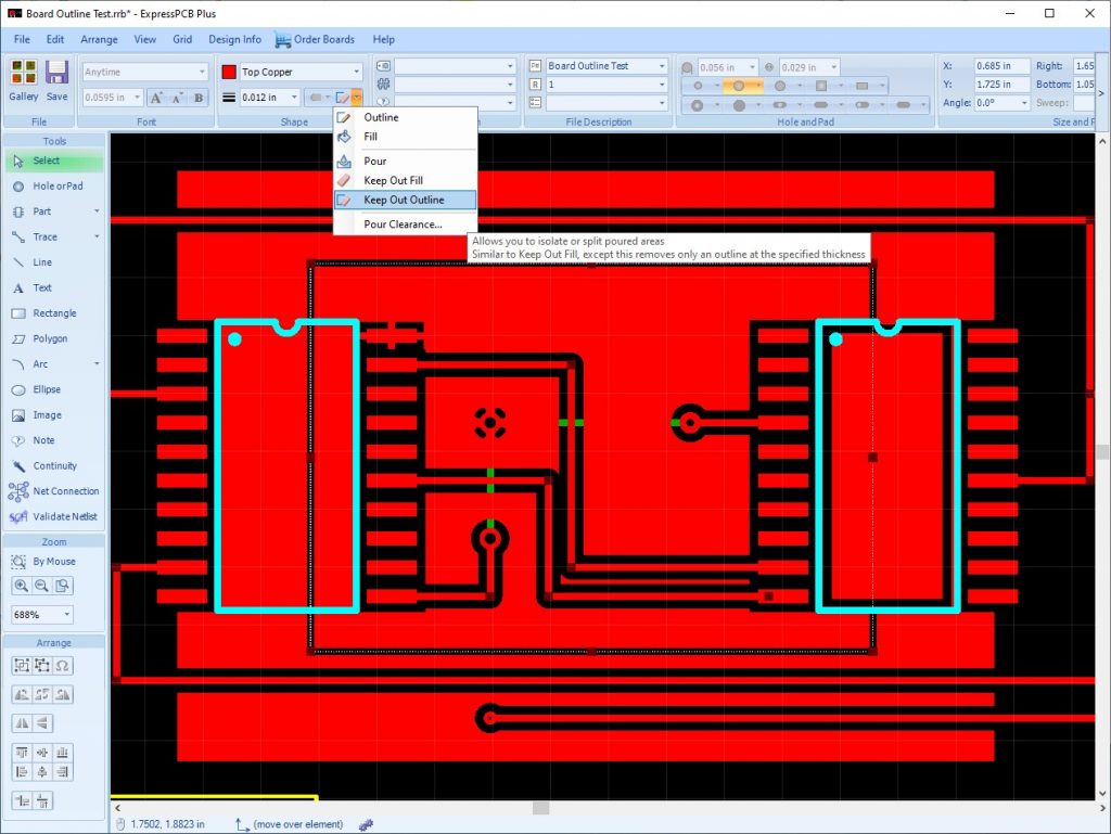
In this example, the Pour Clearance and Pad Connection settings apply to both the interior and exterior. The one item to note when using the “Keep Out Outline” option, are pads that may cross the created “split” and create a short between the two sections of plane as shown below:

It is important to note the inner layers in ExpressPCB Plus can not have the type of pour changed or be deleted. They are based on the Board Edge. If you wish to “remove” the inner layer planes, you can place a rectangle or polygon using “Keep Out Fill” that is similar to your board edge. Please note, you will not be able to place an additional “Poured” area within the Keep Out Fill. You would need to modify the Keep Out Fill to allow areas with the attributes of the original pour.
Additionally, the View Menu – Show Pours setting only changes the appearance of your on screen view. This does not remove, or alter any of the fills/pours found in your design. A good general rule is to set the Show Pours to “All”, and review your design. How the board is displayed on screen, is how the copper will be manufactured. If you feel a different Pour option may be needed, you can select your rectangle, polygon, arc, or ellipse and simply change the Pour option to see how it affects your design without having to redraw the defined area.
We hope this helps to better understand the options available for copper pours in ExpressPCB Plus. If you have any additional questions, you can contact our support staff either by mailing support@expresspcb.com, or using the Live Chat available on our website. Thank you for choosing ExpressPCB as your PCB design software and manufacturing partner.
